Class 12 PCB . Physics . Physics Part II . Semiconductor Electronics Materials Devices and Simple Circuits
Chapter 6: Semiconductor Electronics: Materials, Devices And Simple Circuits
Ch 6
Physics
Class 12 PCB
Introduction
Electronic Devices and Vacuum Tubes
Electronic device — A device that controls the flow of electrons and forms a basic building block of electronic circuits.
Vacuum Tubes (Valves)
- Before 1948: Electronic circuits mostly used vacuum tubes, also called valves, before the discovery of the transistor.
- Vacuum diode: Has two electrodes: a cathode and an anode, often called the plate.
- Triode: Has a cathode, plate and grid; a tetrode and pentode have four and five electrodes, respectively.
- Electron supply and control: A heated cathode supplies electrons; voltage between electrodes controls their flow through the vacuum.
- One-way flow: Electrons flow only from the cathode to the anode, giving these devices their valve-like action.
Limitations of Vacuum Tubes
- Vacuum requirement: The space between electrodes must be evacuated; otherwise, electrons may lose energy in collisions with air molecules.
- Practical drawbacks: Vacuum tubes are bulky, consume high power, generally operate at high voltages (about ), and have limited life and low reliability.
Semiconductor Electronics
Semiconductor device — A solid-state device that controls charge carriers moving within a semiconductor.
Features and Advantages
- Control of carriers: Light, heat or a small applied voltage can change the number of mobile charges in a semiconductor.
- Solid-state operation: Charge carriers are supplied and move within the solid; no heated cathode or large evacuated space is needed.
- Advantages: Semiconductor devices are small, consume low power, operate at low voltages, and have long life and high reliability.
- Display technology: Cathode ray tubes (CRTs) in televisions and computer monitors are being replaced by liquid crystal display (LCD) monitors with supporting solid-state electronics.
| Feature | Vacuum tubes | Semiconductor devices |
|---|---|---|
| Where carriers move | Through an evacuated space | Within the solid |
| Carrier supply | Heated cathode | Mobile charges in the semiconductor |
| Operating needs | Vacuum and generally high voltage | No large evacuated space; low voltage |
| Size, power and reliability | Bulky, high power, limited life and low reliability | Small, low power, long life and high reliability |
Early Semiconductor Application
- Galena detector: A naturally occurring galena crystal () with a metal point contact was used to detect radio waves, before the full potential of semiconductor devices was understood.
Development of Semiconductor Electronics
- 1930sIt became clear that semiconductors and their junctions could control the number and direction of charge carriers.
- 1948The transistor was discovered; before this, electronic circuits mostly relied on vacuum tubes.
Devices and Circuits in This Chapter
- Junction diode: A semiconductor device with two electrodes.
- Bipolar junction transistor: A semiconductor device with three electrodes.
- Applications: The chapter also introduces circuits that demonstrate uses of these devices.
Why are semiconductor devices more practical than vacuum tubes?
Quick recap
- Vacuum tubes control electron flow through a vacuum using a heated cathode and electrode voltages.
- Electrons flow from cathode to anode in a vacuum tube, giving it valve-like action.
- Semiconductors control mobile charge carriers within a solid; light, heat or small voltages can affect their number.
- Compared with vacuum tubes, semiconductor devices are smaller, lower-power, lower-voltage, longer-lasting and more reliable.
- A galena crystal () with a metal point contact was used as an early radio-wave detector.
- This chapter introduces junction diodes, bipolar junction transistors and circuits using them.
Classification Of Metals,Conductors And Semiconductors
Classification by Electrical Conductivity
- Classification: Solids are grouped by their electrical conductivity or resistivity.
- Key distinction: Metals conduct well, insulators conduct very poorly, and semiconductors have intermediate conductivity.
Types of Semiconductors
| Type | Examples |
|---|---|
| Elemental | Silicon (), germanium () |
| Compound—inorganic | , , , |
| Compound—organic | Anthracene, doped phthalocyanines |
| Semiconducting polymers | Polypyrrole, polyaniline, polythiophene |
Materials used in this chapter
- Common devices: Most available devices are based on elemental semiconductors ( or ) and inorganic compound semiconductors.
- Organic materials: Devices using organic semiconductors and semiconducting polymers began emerging after 1990, supporting polymer-electronics and molecular-electronics.
- Scope: This chapter focuses on inorganic semiconductors, especially and ; the general ideas also apply broadly to compound semiconductors.
Energy Bands in Solids
Bands in Silicon and Germanium
- Outer electrons: Each or atom has four outer-shell electrons; the outer shell is for and for .
- For atoms: The crystal has valence electrons and available outer-shell energy states.
- Band splitting: In and crystals, these states split into two bands with states each, separated by an energy gap.
- At : The valence band is completely filled by the electrons, while the conduction band is empty.
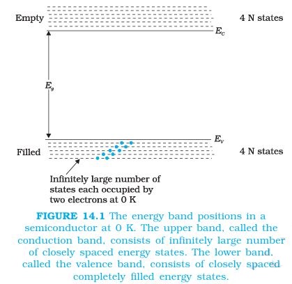
Energy band gap — The energy band gap is the energy difference between the bottom of the conduction band and the top of the valence band: .
Band-Based Classification of Solids
| Material | Band arrangement | Why it conducts or does not conduct |
|---|---|---|
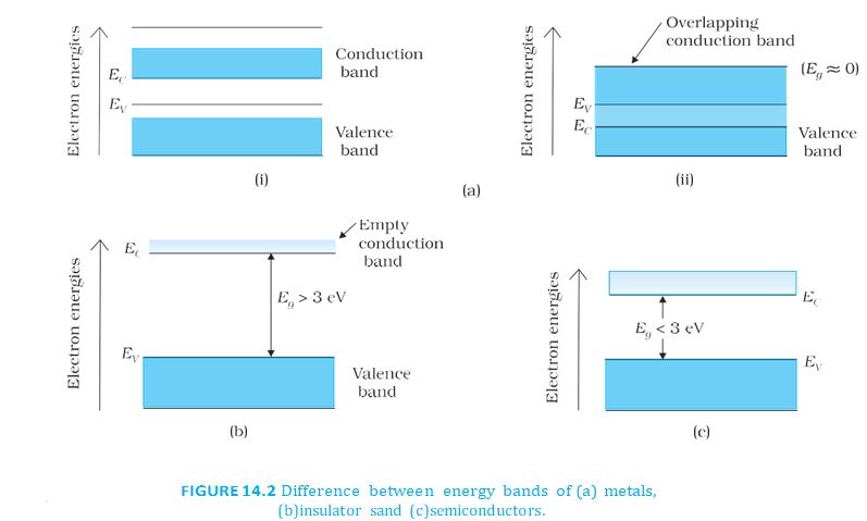
| Metal | The conduction band is partially filled while the valence band is partially empty, or the conduction and valence bands overlap. | In a partially filled band, electrons can move into nearby vacant states. With overlap, valence-band electrons can enter the conduction band. Both arrangements provide many mobile electrons, so conductivity is high. |
| Insulator | A large gap, typically , separates the filled valence band from the empty conduction band. | Thermal energy does not readily excite electrons across the gap, so electrical conduction is negligible. |
| Semiconductor | A finite but small gap, typically , separates the valence and conduction bands. | At room temperature, some electrons gain enough energy to enter the conduction band. Their small number makes resistance lower than in insulators, but conductivity remains below that of metals. |
How can a metal conduct if its conduction band does not overlap the valence band?
What charge carriers are produced when a semiconductor electron enters the conduction band?
Quick recap
- Metals have high conductivity, semiconductors intermediate conductivity, and insulators very low conductivity.
- Semiconductors may be elemental or compound; important elemental examples are and .
- Closely spaced electron energy levels form bands: the valence band and conduction band.
- In and , the valence band is full and the conduction band empty at .
- The band gap separates the two bands and helps determine electrical behaviour.
- Metals have a partially filled band with a partially empty valence band, or overlapping bands; small gaps permit thermal excitation while large gaps inhibit it.
Intrinsic Semiconductor
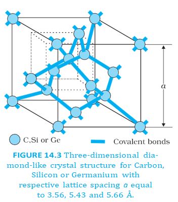
Crystal Structure and Covalent Bonds
Thermal Generation of Electrons and Holes
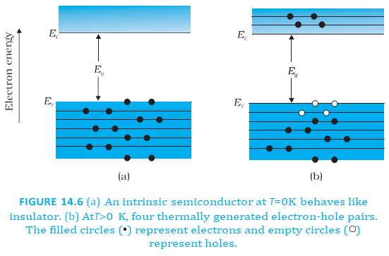
- Thermal excitation: In silicon and germanium, heat can free some covalently bonded electrons.
- Electron–hole pairs: Each freed electron leaves a vacancy called a hole; both can contribute to conduction.
Motion of Charge Carriers and Current
A hole is not a separate particle moving through the crystal: its motion describes the successive movement of bound electrons into vacant bonds.
Generation, Recombination and Equilibrium
- Generation: Thermal energy creates conduction electrons and holes in pairs.
- Recombination: A conduction electron can recombine with a hole, removing both mobile carriers.
- Equilibrium: At equilibrium, the rates of carrier generation and recombination are equal.
Intrinsic Semiconductor Energy Bands
Why Carbon Is an Insulator but Silicon and Germanium Are Semiconductors
Why does an intrinsic semiconductor have equal numbers of electrons and holes?
Why is carbon an insulator while silicon and germanium are intrinsic semiconductors?
Quick recap
- Structure: Si and Ge form diamond-like crystals with four covalent bonds per atom.
- Thermal generation: A freed electron and the hole it leaves form an electron–hole pair.
- Intrinsic carriers: in a pure semiconductor.
- Current: Electrons and holes both contribute: .
- Equilibrium: The generation rate equals the recombination rate.
- Temperature and material: At an intrinsic semiconductor behaves as an insulator; Ge and Si have smaller energy gaps than carbon.
Extrinsic Semiconductor
Doping and Extrinsic Semiconductors
Extrinsic semiconductor — A semiconductor whose conductivity is increased by deliberately adding a small, controlled amount of impurity.
Doping
- Need: Intrinsic Si and Ge have very low conductivity at room temperature; adding suitable impurities raises conductivity greatly.
- Doping: The deliberate addition of a desirable impurity is called doping; the added atoms are dopants.
- Lattice: Dopants replace only a few semiconductor atoms, so their atomic size should be nearly the same as Si or Ge to avoid distorting the crystal.
- Concentration: Doping is typically at a few parts per million (ppm).
| Dopant type | Valency | Examples |
|---|---|---|
| Pentavalent | Arsenic (As), antimony (Sb), phosphorus (P) | |
| Trivalent | Indium (In), boron (B), aluminium (Al) |
n-Type Semiconductor
n-type semiconductor — An extrinsic semiconductor doped with pentavalent impurities, in which electrons are the majority carriers.
Donor action
- Bonding: A pentavalent atom substitutes for Si or Ge; four of its valence electrons form covalent bonds with neighbouring atoms.
- Extra electron: The fifth electron is weakly bound and needs little energy to become free; the impurity donates one conduction electron and is called a donor.
- Ionisation energy: It is about in Ge and in Si, much less than the intrinsic band gap.
- Donor core: After donating its electron, the donor remains as a fixed positive ion in the lattice.
- Temperature: The number of donor-supplied conduction electrons depends strongly on the doping level and is independent of any increase in ambient temperature; intrinsic carriers increase weakly with temperature.
Electrons are the majority carriers; holes are the minority carriers.
p-Type Semiconductor
p-type semiconductor — An extrinsic semiconductor doped with trivalent impurities, in which holes are the majority carriers.
Acceptor action
- Incomplete bond: A trivalent atom forms covalent bonds with three neighbouring Si or Ge atoms; the fourth bond has a vacancy called a hole.
- Hole movement: A nearby electron can fill the vacancy, leaving a new hole at its former position; the hole therefore moves through the crystal.
- Acceptor: The dopant accepts an electron to complete the bond and becomes an effectively fixed negative ion; each acceptor creates one hole.
- Carrier sources: Holes come from acceptors and intrinsic generation, while conduction electrons are produced intrinsically.
- Charge neutrality: The mobile charge of carriers is balanced by the oppositely charged ionised dopant cores.
Holes are the majority carriers; electrons are the minority carriers.
| Point | n-type | p-type |
|---|---|---|
| Dopant | Pentavalent | Trivalent |
| Impurity role | Donor of an electron | Acceptor of an electron |
| Majority carrier | Electron | Hole |
| Minority carrier | Hole | Electron |
| Impurity ion after action | Positive donor core | Negative acceptor core |
Carrier Concentrations and Equilibrium
- Recombination: Many majority carriers increase the chance that minority carriers meet them and recombine, reducing the minority-carrier concentration.
- n-type: Donor electrons dominate; holes are reduced by recombination.
- p-type: Acceptor-produced holes dominate; intrinsic electrons are reduced by recombination.
- Equilibrium relation: In thermal equilibrium, the product of electron and hole concentrations equals the square of the intrinsic concentration.
Applies to a semiconductor in thermal equilibrium.
Energy Levels in Doped Semiconductors
| Dopant | Energy level | Effect at room temperature |
|---|---|---|
| Donor in n-type | lies just below the conduction-band edge . | Donor electrons need little energy to enter the conduction band. |
| Acceptor in p-type | lies just above the valence-band edge . | Valence electrons move to the acceptor level, leaving holes in the valence band. |
- Ionisation: At room temperature, most donor or acceptor atoms are ionised; impurity states supply most majority carriers.
- Intrinsic carriers: Thermal excitation across the full band gap also creates electron–hole pairs, but usually contributes far fewer carriers than doping.
- Energy direction: With added energy, electrons move to higher energy levels; holes correspondingly move toward lower energy levels.
Band Gaps and Example
| Material | Energy gap |
|---|---|
| Diamond (C) | |
| Silicon (Si) | |
| Germanium (Ge) | About (approximately ) |
| Tin (Sn) | ; it is a metal. |
Band gap and resistivity
- Relationship: The differences in resistivity among diamond, Si and Ge depend on the energy gap between their valence and conduction bands.
Example: 1 ppm Arsenic in Silicon
- Given: Silicon atom density , arsenic concentration , and intrinsic concentration .
- Donor concentration: .
- Electrons: Intrinsic electrons are negligible compared with donor electrons, so .
- Holes: From the mass-action law, .
- Pentavalent donor → extra electrons → n-type.
- Trivalent acceptor → holes → p-type.
- Doping changes carrier concentrations but the crystal remains electrically neutral.
Quick recap
- Doping adds a small, suitable impurity concentration to Si or Ge to increase conductivity.
- Pentavalent dopants donate electrons and produce n-type material; electrons are the majority carriers.
- Trivalent dopants accept electrons and produce holes, making p-type material; holes are the majority carriers.
- Donor-supplied conduction electrons depend on dopant concentration and are independent of an increase in ambient temperature.
- Majority carriers reduce minority-carrier concentration through recombination.
- Donor levels lie just below the conduction band; acceptor levels lie just above the valence band.
- At thermal equilibrium, ; band-gap differences help explain the resistivity differences among C, Si and Ge.
p-n Juncction
Formation of a p–n Junction
p–n junction — The boundary formed between p-type and n-type regions of a semiconductor; it is the basic building block of devices such as diodes and transistors.
How it is formed
- Formation: A small, controlled amount of pentavalent impurity can convert part of a p-type silicon wafer into n-type silicon.
- Boundary: The wafer then has p-type and n-type regions separated by a metallurgical junction.
Diffusion, Drift and the Depletion Region
Carrier movement across the junction
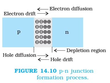
- Concentration gradient: Electrons are more concentrated in the n-region, while holes are more concentrated in the p-region.
- Diffusion: Carriers move from higher to lower concentration: electrons move from n to p, and holes from p to n. This produces diffusion current.
- Fixed ions: Electrons leaving the n-region expose immobile positive donor ions; holes leaving the p-region expose immobile negative acceptor ions.
- Depletion region: These fixed charges form space-charge layers on either side of the junction, depleted of mobile electrons and holes. Its thickness is about .
Drift and equilibrium
- Electric field: The positive charge on the n-side and negative charge on the p-side create a field directed from n to p.
- Drift: This field drives electrons from p to n and holes from n to p, producing drift current opposite to diffusion current.
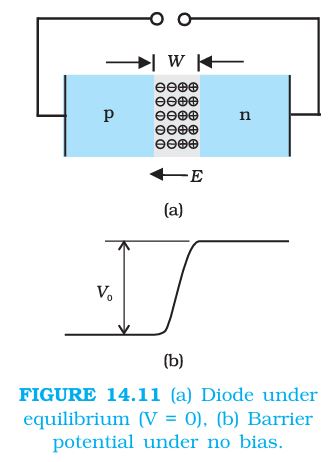
- Establishment of equilibrium: Diffusion initially dominates; as fixed charges build up, the electric field and drift current increase until the two currents balance.
- Equilibrium condition: The net current through an unbiased p–n junction is zero.
| Point | Diffusion current | Drift current |
|---|---|---|
| Cause | Carrier concentration gradient | Electric field in the depletion region |
| Carrier movement | Electrons: n to p; holes: p to n | Electrons: p to n; holes: n to p |
| Direction relative to the other current | Opposite to drift current | Opposite to diffusion current |
The diffusion and drift currents are equal in magnitude and opposite in direction.
Barrier Potential
Barrier potential — The potential difference across a p–n junction that opposes further carrier diffusion and helps establish equilibrium.
- Polarity: As electrons leave the n-region and enter the p-region, the n-region becomes positive relative to the p-region.
- Effect: The resulting potential opposes further electron flow from n to p, helping prevent continued diffusion at equilibrium.
Can a p-type slab and an n-type slab simply be physically joined to make a p–n junction?
Quick recap
- Junction formation: A p–n junction is the boundary between p-type and n-type regions in one semiconductor crystal.
- Diffusion: Electrons move n to p and holes p to n because of concentration gradients.
- Depletion: Diffusion leaves fixed positive donor ions on the n-side and fixed negative acceptor ions on the p-side.
- Drift: The depletion-region electric field drives electrons p to n and holes n to p, opposite to diffusion.
- Equilibrium: Drift and diffusion currents balance, giving zero net current.
- Barrier potential: The n-region is positive relative to the p-region; this potential opposes further carrier diffusion.
Semiconductor Diode
Structure and Function of a Diode
Semiconductor diode — A two-terminal device consisting of a p–n junction with metallic contacts; it conducts mainly in one direction.
Junction and barrier
- Majority carriers: Holes are the majority carriers in the p-type region; electrons are the majority carriers in the n-type region.
- Depletion region: Electrons and holes recombine near the junction, leaving very few mobile carriers and fixed ions; this region contains an electric field.
- Barrier potential: The junction’s electric field opposes further carrier movement across it; an external voltage can alter the barrier.
- Symbol: The conventional direction of forward current is from the p-side to the n-side.
Forward Bias
Forward bias — A diode is forward biased when its p-side is connected to the battery’s positive terminal and its n-side to the negative terminal.
Effect of forward bias
- Voltage drop: Most applied voltage falls across the high-resistance depletion region; the drops across the p- and n-regions are negligible.
- Barrier and width: The applied voltage opposes the built-in potential, reducing the barrier height and depletion-layer width.
- Effective barrier: For applied voltage , the effective barrier is .
- Current: A small applied voltage produces a small current; increasing the voltage lowers the barrier further, so more carriers cross and current increases.
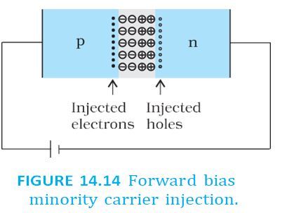
Minority-carrier injection — Under forward bias, electrons cross from n to p and holes cross from p to n, becoming minority carriers on the opposite sides.
Forward current
- Diffusion: Injected electrons diffuse away from the junction through the p-side; injected holes diffuse away through the n-side.
- Total current: Hole-diffusion current and conventional current due to electron diffusion add together; forward current is usually measured in mA.
Reverse Bias
Reverse bias — A diode is reverse biased when its n-side is connected to the battery’s positive terminal and its p-side to the negative terminal.
Effect of reverse bias
- Barrier and width: Applied voltage acts in the same direction as the built-in potential, increasing the barrier and widening the depletion region.
- Effective barrier: For applied voltage , the effective barrier is .
- Diffusion current: The increased barrier strongly suppresses electrons moving from n to p and holes moving from p to n.
- Drift current: The junction field sweeps minority carriers across the junction towards their majority-carrier regions; this current is typically a few μA.
- Bias comparison: Drift current also exists under forward bias, but is negligible compared with the much larger injected-carrier current.
Reverse saturation and breakdown
- Reverse saturation current: Before breakdown, reverse current is very small (usually in the μA range) and nearly independent of applied voltage; its size is limited mainly by the available minority carriers.
- Breakdown voltage: At the critical reverse voltage , reverse current rises sharply; a small further voltage increase can cause a large current increase.
- Current rating: An external circuit must limit current. Excess reverse or forward current can overheat and destroy the diode.
Diode V–I Characteristics
Characteristic curve
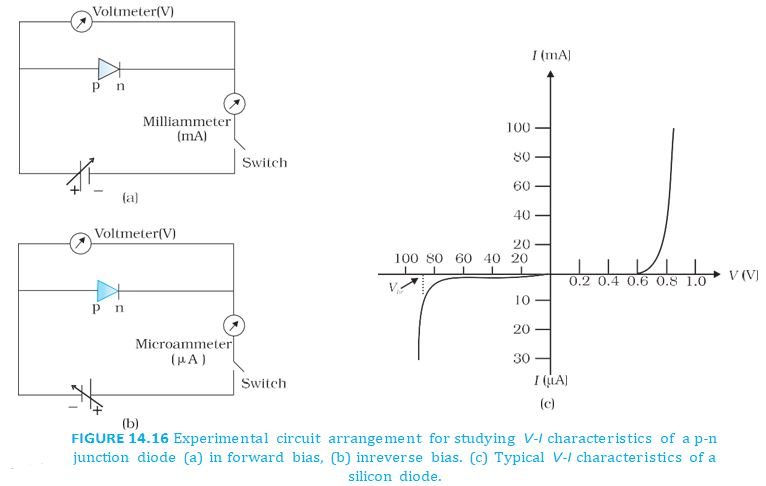
- Measurement: A potentiometer or rheostat varies the diode voltage; current is measured for each voltage.
- Meters: A milliammeter measures the larger forward current; a microammeter measures the small reverse current.
- Forward curve: Current rises rapidly with forward voltage; for a silicon diode, this happens near .
- Reverse curve: Current remains very small and nearly constant before breakdown, then rises sharply at .
- Rectification: Forward resistance is low compared with reverse resistance, allowing a diode to rectify AC voltages.
For a small change in voltage and the corresponding change in current, use this ratio.
From the graph, between at and at , the resistance near is approximately:
At , the graph gives a reverse current of about ; the resistance magnitude is:
Why does a diode conduct strongly in forward bias but only weakly in reverse bias?
What happens at the breakdown voltage of a diode?
Quick recap
- A p–n diode is a two-terminal junction device with a depletion region and barrier potential.
- Holes are majority carriers in p-type material; electrons are majority carriers in n-type material.
- Forward bias connects p to positive and n to negative; it lowers the barrier and produces a large current.
- Reverse bias connects n to positive and p to negative; it raises the barrier and produces a small minority-carrier drift current.
- Reverse saturation current is nearly voltage-independent until breakdown at .
- Diode V–I curves show low forward resistance and high reverse resistance; excessive current can damage the diode.
- Dynamic resistance is .
Application Of Juction Diode As A Rectifier
Rectification
- Rectification: A diode’s low forward resistance and high reverse resistance allow current mainly in one direction.
- Result: Applying an alternating voltage to a diode circuit produces a one-directional, pulsating output.
Half-Wave Rectifier
- Operation: A half-wave rectifier uses one diode in series with a load to pass one half-cycle of the AC input.
- Output: The load receives pulsating voltage in one direction, with no appreciable output during the opposite half-cycle.
Full-Wave Rectifier
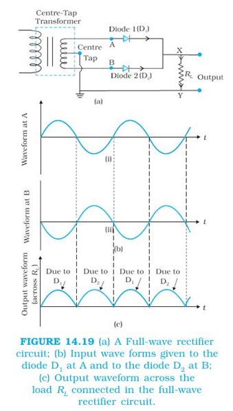
| Point | Half-wave | Full-wave |
|---|---|---|
| Input half-cycles used | One | Both |
| Centre-tapped transformer | Not required | Required in the two-diode arrangement |
| Rectification | Less effective | More effective because output is obtained during both half-cycles |
Another Full-Wave Arrangement
- Four-diode circuit: A full-wave rectifier can also be made with four diodes and does not need a centre-tapped transformer.
Capacitor Filter
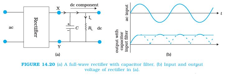
The time constant of the capacitor-load circuit is the product of the capacitance and effective load resistance.
Why is a two-diode centre-tap circuit called a full-wave rectifier?
How does a capacitor filter smooth rectifier output?
Quick recap
- A diode rectifies AC because it conducts in forward bias and blocks in reverse bias.
- A half-wave rectifier gives output during one input half-cycle only.
- A centre-tap full-wave rectifier uses two diodes alternately to produce output during both half-cycles.
- A four-diode full-wave rectifier does not require a centre-tapped transformer.
- A capacitor charges near output peaks and discharges through the load between peaks to smooth the output.
- The time constant is ; increasing it slows the capacitor's voltage fall.
Summary & Points To Ponder
Semiconductor Materials
Basic properties
- Semiconductors are the basic materials used in solid-state devices such as diodes, transistors and integrated circuits (ICs).
- Material type depends on the lattice structure and the atomic structure of its constituent elements.
- Resistivity is low in metals, very high in insulators, and intermediate in semiconductors.
| Class | Resistivity | Examples |
|---|---|---|
| Metal | to | — |
| Insulator | Greater than | — |
| Semiconductor | Intermediate between metals and insulators | Elemental: Si, Ge; compound: GaAs, CdS |
Intrinsic and Extrinsic Semiconductors
Intrinsic semiconductor — A pure semiconductor in which charge carriers are produced by thermal excitation.
Charge carriers and doping
- Electrons and holes are the charge carriers in semiconductors; a hole is an electron vacancy with effective positive charge.
- Intrinsic material: electron and hole concentrations are equal, .
- Doping introduces a suitable impurity into a pure semiconductor, changing its carrier concentration; the result is an extrinsic semiconductor.
- n-type: electrons are the majority carriers; p-type: holes are the majority carriers.
| Type | Dopant in Si or Ge | Dopant role | Majority carriers |
|---|---|---|---|
| n-type | Pentavalent: As, Sb, P | Donor | Electrons; |
| p-type | Trivalent: B, Al, In | Acceptor | Holes; |
Energy Bands and Conductivity
Bands and energy gap
- Valence band: the lower-energy band; its levels are filled. Conduction band: the higher-energy band; its levels may be empty or partly filled.
- Conductivity: electrons in the conduction band can move through the solid and carry current.
- Energy gap lies between the top of the valence band, , and the bottom of the conduction band, .
- Excitation: heat, light or electrical energy can raise valence-band electrons into the conduction band, changing current.
| Material | Energy gap |
|---|---|
| Metal | |
| Semiconductor | to |
| Insulator |
p-n Junction and Diode
Junction barrier and bias
- p-n junction: the key structure in semiconductor devices. Its depletion layer contains immobile ion cores and is depleted of mobile electrons and holes.
- Barrier potential: the depletion layer creates a potential barrier at the junction.
- Forward bias: connect the p-side to the positive terminal and the n-side to the negative terminal; the barrier decreases and current is comparatively large.
- Reverse bias: the barrier increases, so only a very small current flows.
Rectification
- Diode rectification: a diode restricts alternating current to one direction, producing a unidirectional output.
- Smoothing: a capacitor or suitable filter can be used to obtain a direct voltage from the rectified output.
Points to Ponder
Band diagrams and material defects
- Delocalised bands: and represent band-edge energies spread across the solid, not energy levels located at particular points.
- Straight lines in band diagrams indicate the bottom of the conduction band and the top of the valence band, respectively.
- Elemental semiconductors: Si and Ge are made n-type or p-type by introducing dopant atoms as defects.
- Compound semiconductors: changes in the relative stoichiometric ratio can alter the semiconductor type.
- GaAs example: ideal GaAs has a Ga:As ratio of ; Ga-rich material may be , while As-rich material may be .
- Defects matter: dopants and stoichiometric changes can control semiconductor properties in several ways.
How does forward bias affect a p-n junction?
Why does a semiconductor conduct current?
Quick recap
- Semiconductors have intermediate resistivity and form the basis of many solid-state devices.
- Intrinsic semiconductors have equal electron and hole concentrations; doping creates n-type or p-type material.
- Donor dopants produce n-type material; acceptors produce p-type material.
- The energy gap determines material classification and affects how easily electrons enter the conduction band.
- A p-n junction depletion layer creates a barrier that decreases in forward bias and increases in reverse bias.
- Diodes rectify alternating voltage; filtering can smooth the output into a direct voltage.
- Dopants and stoichiometric defects can control the properties of semiconductor materials.
Physics — ALL CHAPTERS
1
Electric Charges And Fields
2
Electrostatic Potential And Capacitance
3
Current Electricity
4
Moving Charges And Magnetism
5
Magnetism And Matter
6
Electromagnetic Induction
7
Alternating Current
8
Electromagnetic Waves
1
Ray Optics And Optical Instruments
2
Wave Optics
3
Dual Nature Of Radiation And Matter
4
Atoms
5
Nuclei
6
Semiconductor Electronics: Materials, Devices And Simple Circuits