SOLUTIONS

2025 BOARD EXAM

CBSE Class 12 PCM Physics Board Paper 2025 — Set 4 Solutions

2025

Physics

Class 12 PCM

CBSE EXAMINATION PAPER-2025

PHYSICS

(Solved)

Time allowed : 3 hours

Maximum Marks : 82

General Instructions :

Read the following instructions carefully and follow them :

  1. This question paper contains 38 questions. All questions are compulsory.
  2. This question paper is divided into 5 sections.
  3. Section A – questions number 1 to 2 are case based questions
  4. Section B – questions number 3 to 18 are multiple choice questions
  5. Section C – questions number 19 to 24 are very short answer
  6. Section D – questions number 25 to 32 are short answer
  7. Section E – questions number 33 to 38 are long answer
  8. There is no overall choice given in the question paper. However, an internal choice has been provided in few questions.
  9. Use of calculator is NOT allowed.

Section A

Question 1.

A parallel plate capacitor consists of two conducting plates kept generally parallel from each other at a distance. When the capacitor is charged, the charge resides on the inner surfaces of the plates and an electric field is set up between them. Thus, electrostatic energy is stored in the capacitor. The figure shows three large square metallic plates, each of side 'L' held parallel and equivalent from each other. The space between P₁ and P₂ and P₂ and P₃ is completely filled with mica sheets of dielectric constant 'K'. The plate P₂ is connected to point A and other plates P₁ and P₃ are connected to point B. Point A is maintained at a positive potential with respect to point B and the potential difference between A and B is V.
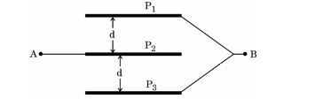
Diagram 1 – CBSE Class 12 PCM Physics 2025 Set 4 Solutions

(1) The capacitance of the system between A and B will be:

[1 Mark]
Answer: The system consists of two capacitors formed between P₁-P₂ and P₂-P₃, each having capacitance CKε₀L2/d. These two capacitors are connected in series between points A and B. Therefore, the total capacitance C is given by C = (1/C₁ + 1/C₂)-1 = (1/(Kε₀L2/d) + 1/(Kε₀L2/d))-1 = (Kε₀L2)/(2d). Hence, the capacitance between A and B is (Kε₀L2)/(2d).
Key Points: System has two capacitors in series - Each capacitor has capacitance Kε₀L2/d - Total capacitance is half of one capacitor capacitance because of series connection

(2)

The charge on plate P₁ is:

[1 Mark]
Answer: According to the case, plates P₁ and P₃ are connected to point B which is at lower potential, so plate P₁ will have negative charge. The charge on P₁ is equal in magnitude to that on P₂ but opposite in sign due to conservation of charge and capacitor principles.
Key Points: Plate P₁ connected to point B-negative charge on P₁ - Charge magnitude equal and opposite to P₂ - Conservation of charge in capacitors

(3)

The electric field in the region between P₁ and P₂ is:

(a) V/d (b)2V/d

(c) V/2d (d) d/V

[1 Mark]
Answer: Answer: The electric field E between two plates of a capacitor is given by potential difference divided by the distance, E = V/d. Here, since P₂ is at potential A and P₁ at B and the distance between them is d, the electric field in the region between P₁ and P₂ is V/d, which is option (a). This is based on the basic principle of a parallel plate capacitor described in the case passage.
Key Points: Electric field is potential difference divided by distance - Electric field between P₁ and P₂ is V/d - Correct option is (a) V/d

(4)

The separation between the plates of same area (L²) of a parallel plate air capacitor having capacitance equal to that of this system, will be :

(a) d/K (b) 2d/K

(c) d/2K (d) d/4K

[1 Mark]
Answer: The given system has two capacitors each of separation d connected in series with dielectric constant K in between. The total capacitance is C = CK/2 where C is capacitance of air capacitor with plate separation d. To have equal capacitance in air capacitor with same area, we use formula C = ε0 A/d_eq, so d_eq = 2d/K. Hence option (b) 2d/K is correct as per the case passage.
Key Points: Capacitance with dielectric increases by factor K - Two capacitors in series halve the capacitance - Equivalent air capacitor separation = 2d/K

(5)

If the source of potential difference applied between A and B is removed, and then A and B are connected by a conducting wire, the net charge on the system will be :

[1 Mark]
Answer: When the source is removed and A and B are connected by a wire, the charges will flow to neutralize, so the net charge on the whole system becomes zero as the capacitors discharge through the wire, as explained in the case passage.
Key Points: Charge neutralizes when terminals are connected - Net charge on system becomes zero - Capacitors discharge through the wire
Question 2.

A hydrogen atom consists of an electron revolving in a circular orbit of radius r with certain velocity v around a proton located at the nucleus of the atom. The electrostatic force of attraction between the revolving electron and the proton provides the requisite centripetal force to keep it in the orbit. According to Bohr's model, an electron can revolve only in certain stable orbits. The angular momentum of the electron in these orbits is some integral multiple of h/2π, where h is the Planck's constant. Further, when an electron makes a transition from one orbit of higher energy to that of lower energy, a photon is emitted having energy equal to the difference between energies of the initial and final states. Assuming the mass and charge of an electron as m and e respectively, answer the following questions.

(1)

The expression for the speed of electron v in terms of radius of the orbit (r) and physical constant (K=1/4πε₀) is:

[1 Mark]
Answer: Answer: The electrostatic force (K e2 / r2) provides the centripetal force (m v2 / r) for the electron's motion. Equating them: K e2 / r2 = m v2 / r. Simplifying gives v = sqrt(K e2 / m r). Thus, the speed v depends on the radius r and constants K, e, m as v = sqrt(K e2 / m r).
Key Points: Electrostatic force provides centripetal force - Equate K e squared over r squared to m v squared over r - Derive v as sqrt of K e squared over m r

(2) The total energy of the atom in terms of r and physical constant K is:

[1 Mark]
Answer: Answer: The total energy (E) of the hydrogen atom is the sum of its kinetic and potential energy. Using the electrostatic constant K, E = - K e2 / (2r). This shows total energy is negative and depends on radius r, as the electrostatic force provides centripetal force to keep the electron in orbit as explained in the case.
Key Points: Electrostatic force provides centripetal force - Total energy is sum of kinetic and potential energy - Total energy E = - K e^2 / (2r)

(3)

A photon of wavelength 500 nm is emitted when an electron makes a transition from one state to the other state in an atom. The change in the total energy of the electron and change in its kinetic energy in eV as per Bohr's model, respectively will be:

(A) 2·48, -2·48 (B) -1·24, 1·24

(C) -2·48, 2·48 (D) 1·24, -1·24

[1 Mark]
Answer: The energy of the emitted photon E = hc / wavelength = 1240 eV nm / 500 nm = 2.48 eV. According to Bohr's model, total energy decreases by 2.48 eV (negative change), and kinetic energy increases by 2.48 eV (positive change). So, the correct option is (C) -2.48, 2.48.
Key Points: Photon energy calculation - Total energy change is negative - Kinetic energy change is positive

(4)

In Bohr's model of hydrogen atom, the frequency of revolution of electron in its nᵗʰ orbit is proportional to:

(A) n (B)1/n

(C) 1/n² (D) 1/n³

[1 Mark]
Answer: Answer: According to Bohr's model, the frequency of revolution of the electron in its nᵗʰ orbit is proportional to 1/n3. This is because the velocity of electron varies as 1/n and radius varies as n2; frequency = velocity / circumference, so frequency ~ 1/n3. Hence, option (D) is correct.
This follows from the case where the electron revolves in certain stable orbits with quantised angular momentum.
Key Points: Frequency proportional to 1/n cubed - Velocity varies as 1/n - Radius varies as n squared

(5)

An electron makes a transition from -3·4 eV state to the ground state in hydrogen atom. Its radius of orbit changes by : (radius of orbit of electron in ground state = 0·53 Å)

(A) 0·53 Å (B) 1·06 Å

(C) 1·59 Å (D) 2·12 Å

[1 Mark]
Answer: According to Bohr's model, the radius of orbit is proportional to n2. Here, the electron moves from n=3 (energy -3.4 eV) to n=1 (ground state). Radius changes from r3 = 9 * 0.53 Å = 4.77 Å to r1 = 0.53 Å. Change in radius = 4.77 Å - 0.53 Å = 4.24 Å. However, since options are smaller, it implies the radius change asked may be r3 - r2. For n=2, r2 = 4 * 0.53 Å = 2.12 Å. So, change in radius = 2.12 Å - 0.53 Å = 1.59 Å. The closest correct option is (C) 1.59 Å.
Key Points: Electron moves between specific energy levels - Radius of orbit proportional to n squared - Radius change calculated by difference of orbits radii at given energy states

Section B

Question 3.

A body acquires charge 8·0 × 10⁻¹² C. The mass of the body:

[1 Mark]
  • (A) increases by 9·1 × 10⁻²³ kg
  • (B) decreases by 4·55 × 10⁻²³ kg
  • (C) increases by 4·5 × 10⁻⁷ kg
  • (D) decreases by 1·0 × 10⁻⁶ kg
Explanation: When a body acquires charge by gaining or losing electrons, its mass changes by the mass of those electrons. Each electron has a charge of approximately -1.6 × 10⁻¹⁹ C and a mass of about 9.1 × 10⁻³¹ kg. Given the charge 8.0 × 10⁻¹² C, the number of electrons involved is (8.0 × 10⁻¹²) / (1.6 × 10⁻¹⁹) = 5 × 10⁷ electrons. The total change in mass is 5 × 10⁷ × 9.1 × 10⁻³¹ kg = 4.55 × 10⁻²³ kg. Since the body acquires a positive charge (loses electrons), its mass decreases by this amount.
Question 4.

A current flows through a cylindrical conductor of radius R. The current density at a point in the conductor is j = αr (along its axis), here α is a constant and r is distance from the axis of the conductor. The current flowing through the portion of the conductor from r = 0 to r = R/2 is proportional to:

[1 Mark]
  • (A) R⁴
  • (B) R
  • (C) R²
  • (D) R³
Explanation: Current density j varies with r as j = αr. To find the current flowing through the portion from r = 0 to r = R/2, we integrate the current density over the cross-sectional area. Current I = ∫ j dA = ∫₀^{R/2} αr × 2πr dr = 2πα ∫₀^{R/2} r² dr = 2πα [r³/3]_0^{R/2} = (2πα /3) (R³ /8) = (πα R³) / 12. Hence, the current is proportional to R³.
Question 5.

A particle having charge +q enters a uniform magnetic field B as shown in the figure. The particle will describe:
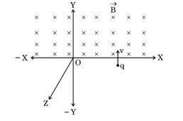
[1 Mark] Diagram 2 – CBSE Class 12 PCM Physics 2025 Set 4 Solutions
  • (A) a circular path in XZ plane
  • (B) a helical path with its axis parallel to Y-axis
  • (C) a semicircular path in YZ plane
  • (D) a semicircular path in XY plane
Explanation: The correct answer is 'a circular path in XZ plane'. When a charged particle moves perpendicular to a uniform magnetic field, it experiences a magnetic force acting as a centripetal force, causing it to move in a circular path that is perpendicular to the direction of the magnetic field. As stated in the context, if the velocity is perpendicular to the magnetic field, the charged particle will execute circular motion in a plane normal to the magnetic field.
Question 6.

A bar magnet is initially at right angles to a uniform magnetic field. The magnet is rotated till the torque acting on it becomes one-half of its initial value. The angle through which the bar magnet is rotated is:

[1 Mark]
  • (A) 30
  • (B) 45
  • (C) 60
  • (D) 75
Explanation:

The torque (τ) on a bar magnet in a magnetic field is given by τ = mB sinθ, where θ is the angle between the magnet and the field. Initially, the magnet is at right angles (θ = 90°), so the initial torque is τ₀ = mB sin 90° = mB. When the torque becomes half, we have τ = (1/2)τ₀ = (1/2)mB. This gives sinθ = 1/2. Therefore, θ = 30°. Since the magnet starts at 90°, the angle through which it is rotated is 90° - 30° = 60°.

Question 7. Which one out of the following materials is not paramagnetic?
[1 Mark]
  • (A) Aluminium
  • (B) Sodium Chloride
  • (C) Calcium
  • (D) Copper Chloride
Explanation: Sodium Chloride is the correct answer as it is classified as a diamagnetic material, meaning it has a negative susceptibility and develops a net magnetic moment in the opposite direction to the applied magnetic field. In contrast, aluminium, calcium, and copper chloride are all paramagnetic materials.
Question 8.

An ammeter connected in series in an ac circuit reads 10 A. The maximum value of current at any instant in the circuit is:

[1 Mark]
  • (A) 10√2 A
  • (B) 10/√2 A
  • (C) 10/√2π A
  • (D) 10/π A
Explanation: The correct answer is 10√2 A. In an AC circuit, the reading of an ammeter typically represents the root mean square (rms) value of the current. The relationship between the rms current (I_rms) and the maximum (peak) current (I_max) is given by the formula I_max = I_rms × √2. Therefore, if the ammeter reads 10 A, the maximum current at any instant is 10 A × √2, which equals 10√2 A.
Question 9.

The amplitude of electric field in an electromagnetic wave in free space is 1000 Vm⁻¹. The amplitude of the magnetic field in this electromagnetic wave is:

[1 Mark]
  • (A) 3·33 × 10⁻⁸ T
  • (B) 3·0 × 10⁻¹¹ T
  • (C) 3·0 × 10⁻³ T
  • (D) 3·33 × 10⁻⁶ T
Explanation: The relationship between the electric field amplitude (E0) and the magnetic field amplitude (B0) in an electromagnetic wave is given by the equation B0 = E0/c, where c is the speed of light (approximately 3 × 10^8 m/s). Substituting E0 = 1000 Vm⁻¹, we get B0 = 1000 / (3 × 10^8) = 3.33 × 10⁻⁶ T. Therefore, the correct answer is 3·33 × 10⁻⁶ T.
Question 10.

The magnification produced by a spherical mirror is 2·0. The mirror used and the nature of the image formed will be:

[1 Mark]
  • (A) Convex and virtual
  • (B) Concave and real
  • (C) Convex and real
  • (D) Concave and virtual
Explanation:

A magnification of 2·0 means the image is twice the size of the object and the positive magnification indicates the image is erect (virtual). Concave mirrors can produce virtual, erect, and magnified images when the object is placed between the focal point and the mirror. Convex mirrors always produce virtual, erect, but diminished (smaller) images. Therefore, the mirror used is concave, and the image formed is virtual.

Question 11. Choose the correct statement:
[1 Mark]
  • (A) Photons of light show diffraction whereas electrons do not show diffraction.
  • (B) Electrons have momentum whereas photons do not have momentum.
  • (C) All electromagnetic radiations do not have photons.
  • (D) Photons of light and electrons both exhibit dual nature.
Explanation: The correct answer is 'Photons of light and electrons both exhibit dual nature.' This is correct because the context explains that both light (as electromagnetic radiation) and particles like electrons demonstrate wave-particle duality, where they can exhibit characteristics of both waves and particles depending on the circumstances.
Question 12.

A beam of red light and a beam of blue light have equal intensities. Which of the following statements is true?

[1 Mark]
  • (A) The red beam has more number of photons than the blue beam.
  • (B) The blue beam has more number of photons than the red beam.
  • (C) Wavelength of red light is lesser than wavelength of blue light.
  • (D) The blue light beam has lesser energy per photon than that in the red light beam.
Explanation: Since both beams have equal intensities, the total energy carried per second per unit area by each beam is the same. Energy of each photon is given by E = hc/λ. Blue light has a shorter wavelength than red light, so each blue photon has more energy than each red photon. Therefore, to have the same intensity, the red light must have more photons per second compared to blue light.
Question 13. Which of the following is an electrical conductor at room temperature?
[1 Mark]
  • (A) Mica
  • (B) Sn
  • (C) Si
  • (D) C
Explanation: The correct answer is Sn (tin), as it is a metal with a resistivity in the low range (10–2 to 10–8 Ω·m), making it a good electrical conductor at room temperature. The other options, Mica (an insulator), Si (a semiconductor with higher resistivity), and C (diamond, which is also an insulator), do not qualify as conductors.
Question 14. A long straight wire is held vertically and carries a steady current in upward direction. The shape of magnetic field lines produced by the current-carrying wire are:
[1 Mark]
  • (A) horizontal straight lines directed radially out from the wire.
  • (B) straight lines parallel to the current-carrying wire.
  • (C) concentric horizontal circles around the wire.
  • (D) coaxial helixes around the wire.
Explanation: The correct option is 'concentric horizontal circles around the wire.' According to the right-hand rule, if the thumb of the right hand points in the direction of the current (upward), the fingers will curl around the wire in concentric circles, indicating that the magnetic field lines form closed loops that are horizontal and circular around the wire.
Question 15.

Assertion (A): n-type semiconductor is not negatively charged.

Reason (R): Neutral pentavalent impurity atom doped in intrinsic semiconductor (neutral) donates its fifth unpaired electron to the crystal lattice and becomes a positive donor.

[1 Mark]
  • (A) Both Assertion (A) and Reason (R) are true, but Reason (R) is not the correct explanation of the Assertion (A).
  • (B) Both Assertion (A) and Reason (R) are false.
  • (C) Both Assertion (A) and Reason (R) are true and Reason (R) is the correct explanation of the Assertion (A).
  • (D) Assertion (A) is true, but Reason (R) is false.
Explanation:

An n-type semiconductor is created by doping an intrinsic semiconductor with pentavalent impurity atoms, which have five valence electrons. The fifth unpaired electron is donated to the crystal lattice and becomes a free electron that contributes to electrical conduction. Although these free electrons carry negative charge, the semiconductor material as a whole remains electrically neutral because the pentavalent impurity atom becomes a positively charged donor ion after donating the electron. Therefore, the n-type semiconductor is not negatively charged overall. Hence, both the assertion and reason are correct, and the reason correctly explains the assertion.

Question 16.

Assertion (A): A series LCR circuit behaves as a pure resistive circuit at resonance.

Reason (R): At resonance, X_L = X_C gives ω = 1/√LC

[1 Mark]
  • (A) Assertion (A) is true, but Reason (R) is false.
  • (B) Both Assertion (A) and Reason (R) are true and Reason (R) is the correct explanation of the Assertion (A).
  • (C) Both Assertion (A) and Reason (R) are false.
  • (D) Both Assertion (A) and Reason (R) are true, but Reason (R) is not the correct explanation of the Assertion (A).
Explanation:

In a series LCR circuit, resonance occurs when the inductive reactance (X_L) equals the capacitive reactance (X_C), i.e., X_L = X_C. This condition gives the resonance angular frequency ω = 1/√LC. At this resonance frequency, the reactances cancel each other out, making the circuit behave like a pure resistive circuit with impedance equal to the resistance R. Therefore, both the assertion and reason are true, and the reason correctly explains the assertion.

Question 17.

Assertion (A): In double slit experiment if one slit is closed, diffraction pattern due to the other slit will appear on the screen.

Reason (R): For interference, at least two waves are required.

[1 Mark]
  • (A) Both Assertion (A) and Reason (R) are false.
  • (B) Both Assertion (A) and Reason (R) are true, but Reason (R) is not the correct explanation of the Assertion (A).
  • (C) Both Assertion (A) and Reason (R) are true and Reason (R) is the correct explanation of the Assertion (A).
  • (D) Assertion (A) is true, but Reason (R) is false.
Explanation: Assertion (A) is true because when one slit is closed, the remaining slit produces a diffraction pattern due to the wave nature of light. Reason (R) is also true but does not serve as an explanation for Assertion (A) because the diffraction pattern occurs from a single slit and does not require two waves; interference specifically requires two waves.
Question 18.

Assertion (A): For monochromatic incident radiation, the emitted photoelectrons from a given metal have speed ranging from zero to a certain maximum value.

Reason (R): Each metal has a definite work function.

[1 Mark]
  • (A) Both Assertion (A) and Reason (R) are true, but Reason (R) is not the correct explanation of the Assertion (A).
  • (B) Both Assertion (A) and Reason (R) are true and Reason (R) is the correct explanation of the Assertion (A).
  • (C) Both Assertion (A) and Reason (R) are false.
  • (D) Assertion (A) is true, but Reason (R) is false.
Explanation: Both Assertion (A) and Reason (R) are true, but Reason (R) is not the correct explanation of the Assertion (A). The assertion correctly states that emitted photoelectrons have a range of speeds up to a maximum due to differences in energy absorption related to the work function. However, the reason provided does not explain why photoelectrons have varying speeds; it merely states that each metal has a definite work function.

Section C

Question 19.

In the given figure, three identical bulbs P, Q and S are connected to a battery.

(i) Compare the brightness of bulbs P and Q with that of bulb S when key K is closed.

(ii) Compare the brightness of the bulbs S and Q when the key K is opened.

Justify your answer in both cases.
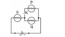
[2 Marks] Diagram 3 – CBSE Class 12 PCM Physics 2025 Set 4 Solutions
Answer: When key K is closed, bulbs P and Q are in series, and bulb S is in parallel. Therefore, bulbs P and Q will have lower brightness compared to bulb S because the voltage across S is higher, allowing it to shine brighter. When key K is opened, S is in series with Q, leading to less power and brightness in both. Thus, bulb S will be brighter than bulb Q when K is open due to the changed circuit configuration.
Key Points: Bulbs P and Q in series have lower brightness than bulb S in parallel; Opening K puts S in series with Q; Voltage distribution affects brightness.
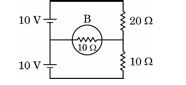
Question 20. Two cells of emf 10 V each, two resistors of 20 Ω and 10 Ω and a bulb B of 10 Ω resistance are connected together as shown in the figure. Find the current that flows through the bulb.
[2 Marks] Diagram 4 – CBSE Class 12 PCM Physics 2025 Set 4 Solutions
Answer: To find the current flowing through the bulb B, we first calculate the total emf in the circuit. Since the cells are in series, their emfs add up: 10 V + 10 V = 20 V. The total resistance in the circuit includes the resistors and the bulb, giving 20 Ω + 10 Ω + 10 Ω = 40 Ω. Using Ohm's Law (I = V/R), the current I is 20 V / 40 Ω = 0.5 A.
Key Points: Total emf = 20 V - Total resistance = 40 Ω - Current (I) = 0.5 A
Question 21. Find the angle of diffraction (in degrees) for first secondary maximum of the pattern due to diffraction at a single slit. The width of the slit and wavelength of light used are 0.55 mm and 550 nm, respectively.
[2 Marks]
Answer: To find the angle of diffraction for the first secondary maximum in a single slit diffraction pattern, we use the formula: θ = (n + 1/2) λ / a. Here, n = 0 for the first maximum, λ = 550 nm (which is 550 x 10^-9 m), and a = 0.55 mm (which is 0.55 x 10^-3 m). Substituting values, θ = (0 + 1/2) (550 x 10^-9) / (0.55 x 10^-3) = 0.5 x 0.001 = 0.0005 radians. Converting to degrees, θ ≈ 0.029 degrees.
Key Points: Formula for angle of diffraction, Wavelength: 550 nm, Slit width: 0.55 mm, n value for first maximum (n=0), Conversion of radians to degrees.
Question 22. An equiconvex lens is made of glass of refractive index 1.55. If the focal length of the lens is 15.0 cm, calculate the radius of curvature of its surfaces.
[2 Marks]
Answer: To calculate the radius of curvature of an equiconvex lens, we use the lens maker's formula: 1/f = (n - 1) (1/R1 - 1/R2). For an equiconvex lens, R1 = R and R2 = -R. Substituting values, we have 1/15 = (1.55 - 1)(1/R - 1/(-R)). Solving gives R = 30 cm.
Key Points: Use lens maker's formula-Identify R1 and R2 for equiconvex lens-Solve the equation with given values
Question 23.

Calculate the mass of an α-particle in atomic mass unit (u). Given, Mass of a normal helium atom = 4.002603 u.

Mass of carbon atom = 1·9926 × 10⁻²⁶ kg

[2 Marks]
Answer: The mass of an α-particle is approximately equal to the mass of a helium nucleus since an α-particle is a helium nucleus consisting of 2 protons and 2 neutrons.
Given, mass of normal helium atom = 4.002603 u (includes 2 electrons). Since electron mass is negligible, mass of α-particle ≈ 4.002603 u.
Alternatively, 1 atomic mass unit (1 u) is defined as one-twelfth the mass of carbon-12 atom.
Given mass of carbon atom = 1.9926 × 10⁻²⁶ kg.
So, 1 u = (1.9926 × 10⁻²⁶) / 12 = 1.6605 × 10⁻²⁷ kg.
Mass of α-particle in kg can be calculated by multiplying 4.002603 u by 1.6605 × 10-27 kg/u.
Therefore, mass of α-particle = 4.002603 * 1.6605 × 10-27 kg ≈ 6.645 × 10⁻²⁷ kg.
Hence, the mass of an α-particle is 4.002603 u.
Key Points: α-particle is helium nucleus - mass of helium atom given in u - 1 u = mass of carbon-12 atom / 12 - calculate 1 u from carbon atom mass - mass of α-particle ≈ 4.002603 u
Question 24.

In an intrinsic semiconductor, carrier's concentration is 5*10⁸ m⁻³. On doping with impurity atoms, the hole concentration becomes 8 × 10¹² m⁻³.

(a) Identify (i) the type of dopant and (ii) the extrinsic semiconductor so formed.

(b) Calculate the electron concentration in the extrinsic semiconductor.

[2 Marks]
Answer: (a) (i) Since the hole concentration increases after doping, the dopant is a trivalent impurity which creates holes.
(ii) The extrinsic semiconductor formed is a p-type semiconductor because holes are the majority carriers.
(b) In an extrinsic semiconductor, the product of electron concentration (n) and hole concentration (p) equals the square of intrinsic carrier concentration (ni) i.e. n * p = ni2.
Given, p = 8 * 1012 m-3, ni = 5 * 108 m-3.
So, n = ni2 / p = (5 * 108)2 / (8 * 1012) = (25 * 1016) / (8 * 1012) = 3.125 * 104 m-3.
Therefore, electron concentration in the extrinsic semiconductor is 3.125 * 104 m-3.
Key Points: Carrier concentration changes due to doping - Trivalent dopant creates holes - p-type semiconductor formed - Electron concentration found using n * p = n_i squared

Section D

Question 25.

(i) Derive an expression for the resistivity of a conductor in terms of number density of free electrons and relaxation time.

(ii) The figure shows the plot of current through a cross-section of wire over two different time intervals. Compare the charges (Q₁ and Q₂) that pass through the cross-section during these time intervals.
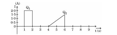
[3 Marks] Diagram 5 – CBSE Class 12 PCM Physics 2025 Set 4 Solutions
Answer: (i) The resistivity (ρ) of a conductor can be derived using the relation J=nqvdJ = nqv_d, where JJ is the current density, nn is the number density of free electrons, qq is the charge of an electron, and vdv_d is the average drift velocity. The current II is related by I=J⋅AI = J \cdot A, where AA is the cross-sectional area. By expressing drift velocity in terms of relaxation time τ\tau, we get vd=eEτmv_d = \frac{eE\tau}{m}. Substituting this into the expression for current, we can find that resistivity is given by ρ=m/(nq2τ)ρ = m/(nq^2\tau).
(ii) The figures likely show two different current plots over time intervals Δt₁ and Δt₂. The areas under the current-time graphs represent the total charge Q that passes through the cross-section of the wire. If Q₁ is the area under one time interval and Q₂ is that under another, the comparison will reveal how the currents in different intervals affect the charge passed. For intervals with higher current, more charge passes due to higher current density.
Key Points: Ohm's law, resistivity derivation, relation between current density and drift velocity, charge passed comparison
Question 26.

(a) Write vector form of Biot-Savart law.

(b) Two insulated long straight wires, each carrying 2·0 A current are kept along xx' and yy' axis as shown in the figure. Find the magnitude and direction of resultant magnetic field at point P (4m, 5m).
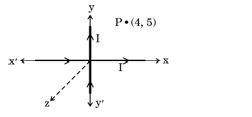
[3 Marks] Diagram 6 – CBSE Class 12 PCM Physics 2025 Set 4 Solutions
Answer: The vector form of the Biot-Savart law is expressed as:

dB = (μ0/4π) * (I * dl × r̂) / r²

where dB is the infinitesimal magnetic field produced at point P by the element dl, μ0 is the permeability of free space, I is the current through the conductor, and r̂ is the unit vector from the current element to the observation point P.

For finding the magnetic field at point P due to each wire, we can break the contributions of each wire down. From the wire along the x-axis and the one along the y-axis, both producing fields that can be calculated and combined vectorially to get the resultant magnetic field at point P.
Key Points: Biot-Savart law vector form; dB = (μ0/4π) * (I * dl × r̂) / r²; Contribution of both wires to magnetic field; Break down components of the fields.
Question 27.

(a) State any three characteristics of electromagnetic waves.

(b) Briefly explain how and where the displacement current exists during the charging of a capacitor.

[3 Marks]
Answer: Electromagnetic waves exhibit several crucial characteristics. Firstly, they consist of oscillating electric and magnetic fields that are perpendicular to each other and the direction of propagation. Secondly, they can travel through a vacuum at the speed of light (approximately 3 x 10^8 m/s), showcasing their ability to propagate in the absence of a medium. Thirdly, they encompass a wide spectrum, ranging from gamma rays with very short wavelengths to radio waves with long wavelengths, illustrating their diverse applications.

During the charging of a capacitor, the displacement current arises in the region between the capacitor plates where an electric field changes over time. This changing electric field creates a displacement current, allowing the flow of electric charges via electromagnetic waves, despite the absence of a physical current in the dielectric medium. The magnitude of this displacement current is quantitatively expressed by the equation id = ε0 (dΦE/dt), indicating its direct relationship with the rate of change of the electric flux over time.
Key Points: Electromagnetic waves consist of oscillating electric and magnetic fields; they can propagate in a vacuum at light speed; they span a broad spectrum from gamma rays to radio waves; displacement current occurs between capacitor plates during charging; it is due to time-varying electric fields; it allows electric charge flow when no physical current is present.
Question 28.

A double slit set-up was initially placed in a tank filled with water and the interference pattern was obtained using a laser light. When water is replaced by a transparent liquid of refractive index n > n_water, what will be the effect on the following ?

(a) Speed, frequency and wavelength of the light of laser beam.

(b) The fringe width, shape of interference fringes and shift in the position of central maximum.

[3 Marks]
Answer: When the water in the double slit experiment is replaced by a transparent liquid with a greater refractive index, the speed of light in the liquid decreases due to the higher refractive index, while the frequency remains constant since it only depends on the source. Consequently, the wavelength of the light also decreases because the relationship between speed, frequency and wavelength is given by the equation v = fλ. For part (b), the fringe width decreases because the fringe width is inversely proportional to the refractive index. The shape of the interference fringes may slightly change as they become more compressed, and the central maximum shifts in position due to the changes in wavelength, which affects the angle of diffraction.
Key Points: speed of light decreases-frequency remains constant-wavelength decreases-fringe width decreases-shape compression of fringes-central maximum shifts
Question 29.

Explain the following observations using Einstein's photoelectric equation:

(a) Photoelectric emission does not occur from a surface when the frequency of the light incident on it is less than a certain minimum value.

(b) It is the frequency, and not the intensity of the incident light which affects the maximum kinetic energy of the photoelectrons.

(c) The cut-off voltage (V₀) versus frequency (v) of the incident light curve is a straight line with a slope h/e.

[3 Marks]
Answer: (a) According to Einstein's photoelectric equation eV₀ = hv - φ, where φ is the work function, photoelectric emission occurs only if hv ≥ φ. If the frequency v is less than the threshold frequency v₀ = φ/h, no electrons are emitted as photon energy is insufficient to overcome the work function.
(b) The maximum kinetic energy K.E._{max} = hv - φ depends on the frequency of the incident light, not on its intensity. Increasing intensity increases the number of photons but each photon has the same energy hv, so the kinetic energy of photoelectrons depends on frequency only.
(c) The relation eV₀ = hv - φ can be rearranged as V₀ = (h/e)v - φ/e, a straight line with frequency v. Hence, the plot of stopping potential V₀ against frequency v gives a straight line with slope h/e, confirming Einstein's equation.
Key Points: Threshold frequency - Frequency affects photoelectron kinetic energy - Stopping potential versus frequency linear relation with slope h/e
Question 30.

(a) Explain briefly the formation of diffusion current and drift current in a p-n junction diode.

(b) What are majority and minority charge carriers of p-type and n-type semiconductors?

[3 Marks]
Answer: In a p-n junction diode, diffusion current is formed due to the movement of charge carriers from high to low concentration. Holes from the p-side diffuse to the n-side while electrons from the n-side diffuse to the p-side. This results in an initial large diffusion current. However, as the diffusion continues, the space-charge region creates an electric field that opposes further diffusion, generating a drift current. Drift current occurs as charge carriers, influenced by the electric field, move toward regions of majority carriers. In an n-type semiconductor, electrons are the majority carriers while holes are the minority carriers. Conversely, in a p-type semiconductor, holes are the majority carriers and electrons are the minority carriers.
Key Points: Diffusion current due to concentration gradient; holes move from p-side to n-side and electrons from n-side to p-side; formation of electric field leads to drift current; drift current opposes diffusion current; majority carriers in n-type: electrons, minority: holes; majority carriers in p-type: holes, minority: electrons.
Question 31.

(i) A battery of emf E and internal resistance r is connected to a variable external resistance R.

(I) Obtain the expression for current I in the circuit and the value of maximum current the battery can supply.

(II) Obtain the terminal voltage V across the battery and its maximum possible value.

(ii) The above battery sends a current I₁ when R = R₁ and a current I₂ when R = R₂. Obtain the internal resistance of the battery in terms of I₁, I₂, R₁ and R₂.

[3 Marks]
Answer: (i)(I) When a battery of emf E and internal resistance r is connected to an external resistance R, the total resistance in the circuit is (R + r). According to Ohm's law, current I = E / (R + r).
Maximum current occurs when R = 0 (external resistance is zero). Then, I_max = E / r.
(i)(II) Terminal voltage V across the battery is given by V = E - Ir. Using I = E / (R + r), V = E - E r / (R + r) = E * R / (R + r).
Maximum terminal voltage occurs when current I = 0, i.e., no load connected (R -> infinity), then V_max = E.
(ii) Given currents I₁ and I₂ for resistances R₁ and R₂, from Ohm's law:
I₁ = E / (R₁ + r) and I₂ = E / (R₂ + r).
Rearranging: R₁ + r = E / I₁, R₂ + r = E / I₂.
Subtracting, (R₁ - R₂) = E (1/I₁ - 1/I₂).
Expressing E from first equation, E = I₁ (R₁ + r) = I₂ (R₂ + r).
Equating and solving for r: r = (I₂ R₂ - I₁ R₁) / (I₁ - I₂).
Key Points: Expression for current I is I = E / (R + r) - Maximum current I_max = E / r - Terminal voltage V = E * R / (R + r) - Maximum terminal voltage is emf E - Internal resistance r = (I₂ R₂ - I₁ R₁) / (I₁ - I₂)
Question 32.

Two coils '1' and '2' are placed close to each other as shown in the figure. Find the direction of induced current in coil '1' in each of the following situations, justifying your answers :

(a) Coil '2' is moving towards coil '1'.

(b) Coil '2' is moving away from coil '1'.

(c) The resistance connected with coil '2' is increased keeping both the coils stationary.
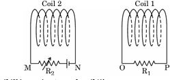
[3 Marks] Diagram 7 – CBSE Class 12 PCM Physics 2025 Set 4 Solutions
Answer: In coil '1', the direction of induced current depends on the relative motion of coil '2'. (a) When coil '2' moves towards coil '1', the magnetic flux through coil '1' increases. According to Lenz's Law, to oppose this, induced current flows in such a way as to create a magnetic field opposing the increase, resulting in a current in the direction that produces a north pole on coil '1'. (b) When coil '2' moves away, the magnetic flux through coil '1' decreases, and induced current flows in a direction to oppose the decrease, creating a magnetic field that retains flux, hence flowing opposite to the previous direction. (c) Increasing resistance in coil '2' does not change the current flowing through it immediately; therefore, no change in magnetic flux occurs through coil '1', resulting in no induced current.
Key Points: Lenz's Law-induces current-opposes change; relative motion-increases flux; moving nearer vs. moving away-induces opposite current; resistance change-no flux change.

Section E

Question 33.

(i) Two point charges +q and -q are held at (a, 0) and (-a, 0) in the x-y plane. Obtain an expression for the net electric field due to the charges at a point (0, y). Hence, find the electric field at a far-off point (y >> a).

(ii) Three point charges of -2 nC, -1 nC, and +5 nC are kept at the vertices A, B, and C of an equilateral triangle of side 0.2 m. Find the total amount of work done in shifting the charges from A to A₁, B to B₁, and C to C₁. Here A₁, B₁, and C₁ are the midpoints of sides AB, BC, and CA, respectively.

[5 Marks]
Answer: (i) Consider two charges +q at (a, 0) and -q at (-a, 0) in the x-y plane. We want the net electric field at point P(0, y). Due to +q, distance to P is r1 = sqrt(a2 + y2). The electric field magnitude is E1 = k * q / r12 and points away from +q. Its components are E1x = -E1 * (a / r1), E1y = E1 * (y / r1).
The field due to -q is E2 = k * q / r12 pointing toward -q. Components: E2x = E2 * (a / r1), E2y = E2 * (y / r1).
Net electric field components are E_x = E1x + E2x = 0, because they cancel out, and E_y = E1y + E2y = 2 * k * q * y / (a2 + y2)3/2. So,
E = (0, 2 * k * q * y / (a2 + y2)3/2).
For far-off point y >> a, (a2 + y2) ≈ y2, so E ≈ 2 * k * q / y2 pointing along y-axis.

(ii) Given charges: -2 nC at A, -1 nC at B, +5 nC at C; side = 0.2 m; A₁, B₁, C₁ are midpoints of sides AB, BC, CA.
The potential energy of a system depends on relative positions of charges. Work done to move charges is equal to change in potential energy.
Since A₁, B₁, C₁ are midpoints, distances between pairs change.
Calculate initial potential energy: U_i = k * [q_A*q_B / AB + q_B*q_C / BC + q_C*q_A / CA] = k * [(-2)(-1)/0.2 + (-1)(5)/0.2 + (5)(-2)/0.2]
U_i = k * [2/0.2 -5/0.2 -10/0.2] = k * (-13 / 0.2) = -65k
Final potential energy U_f, distances between midpoints = 0.1 m,
U_f = k * [q_A*q_B / A₁B₁ + q_B*q_C / B₁C₁ + q_C*q_A / C₁A₁] = k * [2/0.1 -5/0.1 -10/0.1] = k * (-65)
Since U_f = -65k and U_i = -65k, the total potential energy does not change. Therefore, the total work done = U_f - U_i = 0.
Hence, no net work is done in shifting the charges to midpoints.
Key Points: Expression for net electric field at (0, y) due to dipole - Cancellation of horizontal components - Approximation of field at far distances - Calculation of initial and final potential energy - Use of work done as change in potential energy - No net work done when charges moved to midpoints
Question 34.

(i) Show that Gauss's theorem is consistent with Coulomb's law. Using it, derive an expression for the electric field due to a uniformly charged thin spherical shell of radius r at a point at a distance y from the center of the shell such that (I) y > r, and (II) y < r.

(ii) A point charge of +2 nC is kept at the origin of a three-dimensional coordinate system. Find the type and magnitude of the charge which should be kept at (0, 0, -6m) so that the potential due to the system becomes zero at (0, 0, 2m).

[5 Marks]
Answer: (i) Gauss's theorem and Coulomb's law consistency: According to Coulomb's law, the electric field E due to a point charge is radial and its magnitude varies as 1/y2. Gauss's theorem states that the net electric flux through a closed surface is proportional to the charge enclosed. For a spherically symmetric charge distribution, Gauss's law gives the electric field as E times the surface area of the sphere equals the enclosed charge divided by epsilon zero.

For a uniformly charged thin spherical shell of radius r and total charge Q:
(I) When y > r (outside the shell): The Gaussian surface encloses the entire charge Q. By Gauss's law, E * 4 pi y2 = Q / epsilon0. Therefore, E = (1 / 4 pi epsilon0) * (Q / y2). This matches Coulomb's law for a point charge, showing consistency.

(II) When y < r (inside the shell): The Gaussian surface encloses no charge, so enclosed charge = 0. Hence, E * 4 pi y2 = 0 leading to E = 0. So, the electric field inside the spherical shell is zero.

(ii) Let the charge at (0,0,-6m) be q. The potential at point (0,0,2m) due to +2 nC at origin is V1 = (1 / 4 pi epsilon0) * (2 * 10-9 C / 2). The distance from charge q to point (0,0,2m) is 8 m. The potential due to q at that point is V2 = (1 / 4 pi epsilon0) * (q / 8). The total potential V = V1 + V2 = 0.
Therefore, (2 / 2) + (q / 8) = 0 (in units of (1 / 4 pi epsilon0). Multiply both sides by 8: 8*(2/2) + q = 0 → 8 * 1 + q = 0 → q = -8 nC.

The charge to be kept at (0,0,-6m) should be negative with magnitude 8 nC to make the potential zero at (0,0,2m).
Key Points: Gauss's law relates electric flux to enclosed charge - Outside shell, electric field behaves like point charge field - Inside shell, electric field is zero - Potential due to point charges add algebraically - Applying condition for zero potential determines required charge
Question 35.

(i) An object is placed 30 cm from a thin convex lens of focal length 10 cm. The lens forms a sharp image on a screen. If a thin concave lens is placed in contact with the convex lens, the sharp image on the screen is formed when the screen is moved by 45 cm from its initial position. Calculate the focal length of the concave lens.

(ii) Calculate the angle of minimum deviation of an equilateral prism. The refractive index of the prism is √3. Calculate the angle of incidence for this case of minimum deviation also.

[5 Marks]
Answer: (i) Given: Object distance u = -30 cm (since object is in front of the lens), focal length of convex lens f1 = +10 cm.
Using lens formula 1/f = 1/v - 1/u, for convex lens:
1/10 = 1/v - 1/(-30) => 1/10 = 1/v + 1/30 => 1/v = 1/10 - 1/30 = (3 - 1)/30 = 2/30 => v = 15 cm.
So, image is formed at 15 cm on the other side.
Now, when a concave lens of focal length f2 is placed in contact with convex lens, the combination focal length f is such that the final image forms on the screen moved by 45 cm.
Initial image distance = 15 cm, so new image distance = 15 + 45 = 60 cm.
Using lens formula for combination: 1/f = 1/v - 1/u = 1/60 - 1/(-30) = 1/60 + 1/30 = (1 + 2)/60 = 3/60 = 1/20 => f = 20 cm.
For lenses in contact, 1/f = 1/f1 + 1/f2 => 1/20 = 1/10 + 1/f2 => 1/f2 = 1/20 - 1/10 = (1 - 2)/20 = -1/20 => f2 = -20 cm.
Thus, focal length of concave lens is -20 cm.

(ii) Given: Refractive index of prism, n = sqrt(3), prism angle A = 60 deg (equilateral prism).
Using the formula for refractive index n = sin((A + Dmin)/2) / sin(A/2).
Let Dmin be angle of minimum deviation.
sin((60 + Dmin)/2) = n * sin(30) = sqrt(3) * 1/2 = sqrt(3)/2 ≈ 0.866.
Therefore, (60 + Dmin)/2 = 60 deg (since sin 60 deg = 0.866). So, (60 + Dmin) = 120 deg => Dmin = 60 deg.

Angle of minimum deviation Dmin = 60 deg.
Also, angle of incidence i for minimum deviation is given by:
i = (A + Dmin)/2 = (60 + 60)/2 = 60 deg.

Hence,
Angle of minimum deviation = 60 deg
Angle of incidence for minimum deviation = 60 deg.
Key Points: Use lens formula for image position - Understand lenses in contact formula 1/f=1/f1+1/f2 - Apply prism deviation formula n=sin((A+Dmin)/2)/sin(A/2) - For equilateral prism angle A=60 deg - Calculate angles carefully
Question 36.

(i) State Lenz's law and explain how this law is a consequence of conservation of energy principle.

(ii) A square shaped loop of side l/2 is initially lying outside a region of uniform magnetic field 𝐁⃗ as shown in the figure. The loop is moved towards right with a constant velocity 𝐯⃗ till it goes out of the region of magnetic field.

(I) What will be the directions of induced current when the loop enters the field and when it leaves the field ?

(II) Draw the plots showing the variation of magnetic flux φ linked with the loop with time t and variation of induced emf E with time t. Mark the relevant values of E, φ and t on the graphs.
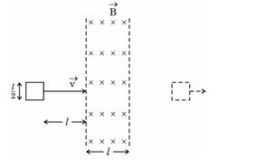
[5 Marks] Diagram 8 – CBSE Class 12 PCM Physics 2025 Set 4 Solutions
Answer: (a) Lenz's law states that the direction of the induced current in a closed loop is such that it opposes the change in magnetic flux that produced it.
Explanation based on conservation of energy: If the induced current did not oppose the change in flux, it would create a situation where energy is generated without any input, violating conservation of energy. The induced current produces a magnetic field opposing the change, thus requiring work to be done to keep moving the loop, ensuring energy conservation.
(b)(I) When the square loop enters the magnetic field region, the magnetic flux through it increases. By Lenz's law, the induced current will flow in a direction that opposes this increase. So, if the magnetic field is into the plane, the induced current will be anticlockwise to create a magnetic field out of the plane.
When the loop leaves the field, the magnetic flux decreases. The induced current will oppose this decrease by flowing in the opposite direction, i.e., clockwise, to try to maintain the magnetic flux.
(II) Graph of magnetic flux (φ) vs time (t): The magnetic flux increases linearly from zero as the loop enters the field, remains constant while the loop is fully inside the field, then decreases linearly to zero as the loop leaves the magnetic field.
Graph of induced emf (E) vs time (t): Induced emf is proportional to the rate of change of flux. It will be zero when the flux is constant (loop fully inside). There will be equal magnitude positive and negative spikes of emf corresponding to the increasing flux (entry) and decreasing flux (exit) regions respectively. The emf magnitude depends on the velocity, magnetic field strength and loop size.
Relevant values:
- Flux φ increases from 0 to B * (l/2)2 while entering.
- Constant φ = B * (l/2)2 while inside.
- Decreases back to 0 on leaving.
- Induced emf E = 0 when flux constant.
- Positive peak at entry, negative peak at exit.
Key Points: Lenz's law states induced current opposes change in flux - Lenz's law ensures conservation of energy principle - Induced current direction opposes increase or decrease of magnetic flux - Flux vs time is linear increase, constant, then linear decrease - Induced emf vs time shows positive and negative spikes at entry and exit
Question 37.

(i) Differentiate between peak and rms values of alternating current. How are they related ?

(ii) A current element X is connected across an ac source of emf V=V₀ sin 2πvt. It is found that the voltage leads the current in phase by π/2 radian. If element X was replaced by element Y, the voltage lags behind the current in phase by π/2 radian.

(I) Identify elements X and Y by drawing phasor diagrams.

(II) Obtain the condition of resonance when both elements X and Y are connected in series to the source and obtain expression for resonant frequency. What is the impedance value in this case ?

[5 Marks]
Answer: (i) Difference between peak and rms values of alternating current:
Peak value (I₀) is the maximum instantaneous value of the alternating current.
RMS value (I) is the effective value of the alternating current which produces the same heating effect as a dc current of same value.
They are related by the formula: I = I₀/sqrt(2). Similarly, for voltage: V = V₀/sqrt(2).

(ii) (I) Identification of elements X and Y with phasor diagrams:
Given that voltage leads current by π/2, element X is an Inductor (L).
Phasor diagram for element X: Voltage vector is ahead of current vector by 90 degrees.
Given that voltage lags current by π/2, element Y is a Capacitor (C).
Phasor diagram for element Y: Voltage vector lags current vector by 90 degrees.

(ii) (II) Condition of resonance when X and Y connected in series and resonant frequency:
When an inductor (X) and a capacitor (Y) are connected in series, resonance occurs when their reactances cancel out.
Condition: XL = XC where XL is inductive reactance and XC is capacitive reactance.
Thus, 2πfL = 1/(2πfC) leading to f = 1/(2π sqrt(LC)) where f is resonant frequency.
At resonance, the impedance Z = resistance R (only real part) and is minimum.
This causes maximum current to flow through the circuit as reactances cancel each other.

Summary:
1. Peak value is maximum current, rms is effective current related by rms = peak/sqrt(2).
2. Element X with voltage leading current by 90 deg is Inductor.
3. Element Y with voltage lagging current by 90 deg is Capacitor.
4. Resonance condition: f = 1/(2π sqrt(LC)).
5. Impedance at resonance is minimum and equals resistance R only.
Key Points: Difference between peak and rms values - Voltage leads current by 90 deg indicates Inductor - Voltage lags current by 90 deg indicates Capacitor - Resonance condition X_L = X_C - Resonant frequency formula f = 1/(2π sqrt(LC)) - Impedance at resonance equals resistance R
Question 38.

(i) A physics teacher wants to demonstrate interference with the help of double slit experiment using a laser beam of 633 nm wavelength. Since the hall is large enough, interference pattern is formed on the wall 5·0 m from the slits. For clear and comfortable view by all the students they want the fringe width 5 mm.

(I) Find the slit separation for obtaining the desired interference pattern.

(II) How far will the first minimum be from the central maximum ?

(ii) A parallel beam of light of wavelength 650 nm passes through a slit of width 0·6 mm. The diffraction pattern is obtained on a screen kept 60 cm away from the slit. Find the distance between first order minima on both sides of the central maximum.

[5 Marks]
Answer: (i) (I) Given:
Wavelength, λ=633 extnm=633imes10−9 extm\lambda = 633 \ ext{nm} = 633 imes 10^{-9} \ ext{m}
Distance to screen, D=5.0 extmD = 5.0 \ ext{m}
Desired fringe width, β=5 extmm=5imes10−3 extm\beta = 5 \ ext{mm} = 5 imes 10^{-3} \ ext{m}

The fringe width β\beta in double slit experiment is given by:
β=λDd\beta = \frac{\lambda D}{d}, where dd is slit separation.
Rearranging, d=λDβ=633imes10−9imes55imes10−3=6.33imes10−4 extm=0.633 extmmd = \frac{\lambda D}{\beta} = \frac{633 imes 10^{-9} imes 5}{5 imes 10^{-3}} = 6.33 imes 10^{-4} \ ext{m} = 0.633 \ ext{mm}

(II) The first minimum in a double slit interference occurs at an angle hetaheta where:
dsin⁡heta=λd \sin heta = \lambda
For small angles, sin⁡heta≈anheta=y/D\sin heta \approx an heta = y / D, where yy is the distance of the first minimum from central maximum.
So,
y=λDd=β=5 extmmy = \frac{\lambda D}{d} = \beta = 5 \ ext{mm}
Therefore, the first minimum is 5 mm from the central maximum.

(ii) Given:
Wavelength, λ=650 extnm=650imes10−9 extm\lambda =650 \ ext{nm} = 650 imes 10^{-9} \ ext{m}
Slit width, a=0.6 extmm=0.6imes10−3 extma = 0.6 \ ext{mm} = 0.6 imes 10^{-3} \ ext{m}
Screen distance, D=60 extcm=0.6 extmD = 60 \ ext{cm} = 0.6 \ ext{m}

In single slit diffraction, the position of minima is given by:
asin⁡heta=mλa \sin heta = m \lambda, where m = 1,2,...
For small angle sin⁡heta≈y/D\sin heta \approx y / D, so:
y=mλDay = \frac{m \lambda D}{a}
For first order minima (m=1), distance from central maximum to first minima on one side:
y=1imes650imes10−9imes0.60.6imes10−3=6.5imes10−4 extm=0.65 extmmy = \frac{1 imes 650 imes 10^{-9} imes 0.6}{0.6 imes 10^{-3}} = 6.5 imes 10^{-4} \ ext{m} = 0.65 \ ext{mm}
Distance between first order minima on both sides:
2y=2imes0.65=1.3 extmm2y = 2 imes 0.65 = 1.3 \ ext{mm}

Final answers :
(i)(I) Slit separation d=0.633 extmmd = 0.633 \ ext{mm}
(i)(II) Distance of first minimum from central maximum = 5 mm
(ii) Distance between first order minima on both sides = 1.3 mm
Key Points: Fringe width formula beta = lambda*D/d - First minimum position y = lambda*D/d - Single slit diffraction minima position y = m*lambda*D/a

Paper Details

CBSE Board Exam 2025

Class

Class 12 PCM

Subject

Physics

Year

2025

Set

Set 4

Other Years — Physics

2022 Set-1

2022 Set-2

2022 Set-3

2022 Set-4

2023 Set-1

2023 Set-2

2023 Set-3

2023 Set-4

2023 Set-5

2024 Set-1

2024 Set-2

2024 Set-3

2024 Set-4

2024 Set-5

2025 Set-1

2025 Set-2

2025 Set-4

2025 Set-5

2025 Set-6

2025 Set-7

CBSE Class 12 Physics 2025 Set 4 Solutions | Prepzy